A Type of Sdram That Can Read or Write Two Words of Data Per Clock Cycle.
SDRAM (Synchronous Dynamic Random Admission Memory):
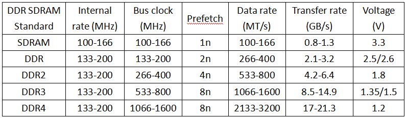
"Synchronous" tells well-nigh the behaviour of the DRAM type. In belatedly 1996, SDRAM began to announced in systems. Unlike previous technologies, SDRAM is designed to synchronize itself with the timing of the CPU. This enables the memory controller to know the exact clock cycle when the requested data will be set, so the CPU no longer has to expect betwixt retentiveness accesses. For example, PC66 SDRAM runs at 66 MT/southward, PC100 SDRAM runs at 100 MT/s, PC133 SDRAM runs at 133 MT/due south, and and then on.
SDRAM can stand for SDR SDRAM (Unmarried Information Rate SDRAM), where the I/O, internal clock and bus clock are the same. For example, the I/O, internal clock and coach clock of PC133 are all 133 Mhz. Single Data Charge per unit means that SDR SDRAM can only read/write ane time in a clock cycle. SDRAM have to wait for the completion of the previous command to exist able to do some other read/write operation.
DDR SDRAM (Double Data Rate SDRAM):
The next generation of SDRAM is DDR, which achieves greater bandwidth than the preceding unmarried data charge per unit SDRAM past transferring data on the rising and falling edges of the clock signal (double pumped). Effectively, information technology doubles the transfer charge per unit without increasing the frequency of the clock. The transfer rate of DDR SDRAM is the double of SDR SDRAM without changing the internal clock. DDR SDRAM, as the kickoff generation of DDR memory, the prefetch buffer is 2bit, which is the double of SDR SDRAM. The transfer charge per unit of DDR is between 266~400 MT/s. DDR266 and DDR400 are of this type.
DDR2 SDRAM(Double Data Rate Ii SDRAM):
Its primary benefit is the ability to operate the external data charabanc twice as fast as DDR SDRAM. This is achieved past improved bus betoken. The prefetch buffer of DDR2 is four bit(double of DDR SDRAM). DDR2 memory is at the same internal clock speed (133~200MHz) as DDR, but the transfer rate of DDR2 tin can achieve 533~800 MT/s with the improved I/O motorbus bespeak. DDR2 533 and DDR2 800 memory types are on the market.
DDR3 SDRAM(Double Information Rate Three SDRAM):
DDR3 retentivity reduces xl% power consumption compared to electric current DDR2 modules, assuasive for lower operating currents and voltages (ane.v V, compared to DDR2'southward 1.eight Five or DDR'southward 2.v V). The transfer rate of DDR3 is 800~1600 MT/due south. DDR3's prefetch buffer width is 8 chip, whereas DDR2's is 4 fleck, and DDR's is 2 bit. DDR3 also adds ii functions, such as ASR (Automatic Self-Refresh) and SRT (Self-Refresh Temperature). They can make the retentivity command the refresh charge per unit co-ordinate to the temperature variation.
DDR4 SDRAM (Double Data Charge per unit Fourth SDRAM):
DDR4 SDRAM provides the lower operating voltage (1.2V) and higher transfer rate. The transfer charge per unit of DDR4 is 2133~3200 MT/s. DDR4 adds four new Banking company Groups engineering science. Each bank grouping has the feature of singlehanded functioning. DDR4 can process 4 data within a clock bicycle, then DDR4'south efficiency is improve than DDR3 apparently. DDR4 too adds some functions, such every bit DBI (Data Bus Inversion), CRC (Cyclic Redundancy Bank check) and CA parity. They can heighten DDR4 retentivity's bespeak integrity, and improve the stability of data transmission/access.
Source: https://www.transcend-info.com/support/faq-296